Pin-to-Reg Timing Analysis
1. Introduction
In Part 4, we covered the reg-to-pin path — a signal leaving an internal FPGA register and driving an external device. That direction is only half of the interface story. The complementary case is the pin-to-reg path: a signal that originates in an external device, enters the FPGA through an input pin, and is captured by an internal register.
The fundamental challenge is the same as before. Vivado can see everything inside the FPGA, but it cannot see the external device or the PCB trace that connects it to the FPGA input pin. The portion of the data path that lies outside the FPGA is invisible to the tool, and without that information the timing analysis is incomplete. The mechanism for supplying that missing information is the set_input_delay constraint.
2. The Pin-to-Reg Path
In a pin-to-reg path, the source register resides in an external device i.e. a memory chip, ADC, sensor, or any other peripheral on the board, while the destination register is inside the FPGA. The data travels from the source register, across the PCB trace, into the FPGA input pin, through internal routing, and is finally captured at the destination register’s data input.
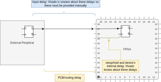
Figure 1: Pin-to-reg path from the external device to the FPGA
3. Input Delay and Why It Is Needed
Vivado models the data path only from the FPGA input pin inward. It has no visibility of:
- The clock-to-output delay of the external source register
- The PCB trace propagation delay from the external device to the FPGA input pin
We supply these values manually through set_input_delay. The constraint value represents the total time elapsed from the shared clock edge to the moment data arrives at the FPGA input pin. It is derived from the external device’s datasheet (for clock-to-output time) and the board layout (for PCB trace delay).
As with all delays, the values vary across process, voltage, and temperature (PVT) corners, so input_delay has both a maximum and a minimum value:
Unlike output_delay_min, which can be negative, input_delay_min is always a positive quantity. Both the external clock-to-output time and the PCB trace delay are inherently positive, so their sum is too.
4. Timing Equations for Pin-to-Reg
4.1 Data Arrival Time
For a pin-to-reg path, Vivado models only the portion of the data path it can see: from the FPGA input pin, through internal routing, to the destination register’s data input. The input delay accounts for everything before that pin. The data arrival time at the destination register is therefore:
\[T_{arrival} = \text{input_delay}_{max} + T_{route,\,int} \tag{3}\]\(T_{route,\,int}\) is the internal routing delay from the FPGA input pin to the destination register. The launch clock path — which runs from the clock source through the external device and back — is entirely outside the FPGA and is not modelled by Vivado. Its effect is fully captured inside the input_delay value.
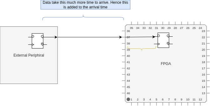
Figure 2: Vivado’s visibility of pin-to-reg paths
4.2 Data Required Time — Setup Analysis
Unlike a reg-to-pin path, where the destination clock is external and Vivado assigns it a delay of zero, in a pin-to-reg path the destination register is inside the FPGA. Vivado therefore has full visibility of the capture clock path, and the clock network delay to the destination register is a real, non-zero quantity in the timing report.
The required time at the destination register’s data input is:
\[T_{required} = T_{clk,\,capture} - T_{su,\,int} - \text{clock uncertainty} \tag{4}\]where $T_{clk,\,capture}$ is the time the capture clock edge arrives at the destination register’s clock pin after travelling through the FPGA clock network, $T_{su,\,int}$ is the setup time of the internal register, and clock uncertainty is the same budget used in reg-to-reg analysis. The setup slack is:
\[\text{Slack}_{setup} = T_{required} - T_{arrival} \geq 0 \tag{5}\]The effect of a large input_delay_max is immediately visible here. It inflates $T_{arrival}$ directly, reducing the available setup slack. A slow external device or a long PCB trace can make it impossible to meet setup timing at the destination register even when the internal routing delay is small.
4.3 Hold Analysis
For hold timing, the minimum delay path is analysed using input_delay_min. The hold check ensures that data does not change too quickly after the capture clock edge — that the data launched by one clock edge does not arrive at the destination register before the register has finished capturing the data from the previous edge.
The hold slack is:
\[\text{Slack}_{hold} = T_{arrival,\,min} - T_{required,\,hold} \geq 0 \tag{6}\]where \(T_{arrival,\,min} = \text{input\_delay}_{min} + T_{route,\,int,\,min}\).
One thing worth noting is that there is no CPR in these equations. That is because CPR removes pessimism from the shared segment of the launch and capture clock paths. Here, the launch clock path is entirely external and invisible to Vivado, so there is no shared segment to optimise. The destination clock is fully modelled, and its delay appears as a non-zero value in the timing report, but that alone is not sufficient to enable CPR.
5. Applying the Constraint in Vivado
The input_delay constraint is applied using the set_input_delay command. As with set_output_delay, it can be written directly into the .xdc file or generated through the Vivado GUI.
The steps are the same as described in Part 4 for reg-to-pin. The only difference is that after opening the timing constraint window in the synthesized design, you select Set Input Delay instead of Set Output Delay.
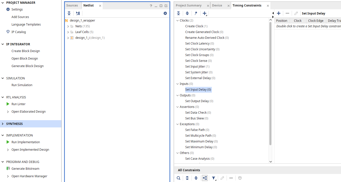
Figure 3: Set Input Delay dialog in Vivado.
In the timing report, input_delay_max is added to the data arrival time in setup analysis, pushing the arrival time later and consuming slack:
And input_delay_min is added to the minimum arrival time in hold analysis:
6. What’s Next
With this post, the core timing analysis series comes to a close. We started with the fundamentals of setup analysis — arrival time, required time, and slack — and progressively worked through clock pessimism removal, hold analysis, and finally the two external interface path types: reg-to-pin and pin-to-reg. Together, these five parts cover the timing analysis model that underlies every path Vivado analyses in a synchronous FPGA design.
The next series will shift focus to clock domain crossing (CDC). Once a design has more than one clock domain, the synchronous timing model no longer applies across domain boundaries, and a different set of techniques is needed — synchronisers, handshake protocols, and FIFOs — each with its own implications for metastability, latency, and throughput. That will be the starting point for the next series.
Series: Understanding FPGA Timing in Vivado
Part Topic Part 1 Setup Analysis Basics — Arrival Time, Required Time, Slack Part 2 Clock Pessimism Removal, Clock Uncertainty & Clock Skew Part 3 Hold Analysis Part 4 Reg-to-Pin Timing & Output Delay Constraints Part 5 (this post) Pin-to-Reg Timing & Input Delay Constraints