Clock Skew, Uncertainty and Pessimism Removal
In Part 1, we covered the basics of setup timing analysis for reg-to-reg paths in Vivado — how to read timing reports, what arrival time and required time mean, and how slack is calculated. We left a few terms unexplained: Clock Pessimism Removal (CPR) and clock uncertainty. In this post, we’ll unpack both of those, along with clock skew, and see how they fit into the timing equations we built up last time.
1. Clock Pessimism Removal (CPR)
It stands for clock pessimism removal. We calculate the reg-to-reg setup time between a source register and a destination register. Now the clock to these registers reaches through different paths, however the source and destination clock can share some path as well.
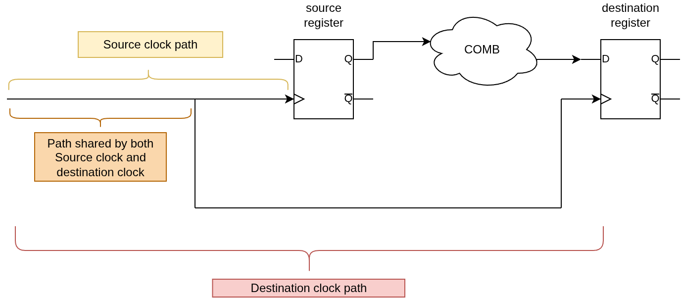 Figure 1: Source, destination, and shared clock paths in a reg-to-reg timing path
Clock signals do not reach flip-flops instantaneously. They pass through intermediate elements in the clock path such as MMCMs, BUFGs, routing resources, and buffers. These elements add a delay between the clock edge generated through the clock source and that clock edge reaching the source/destination register. In the previous blog, we called it clock delay in required and arrival time calculations.
\[\text{Data Arrival Time} = \text{Launch Edge} + \text{Source Clock Delay} + T_{cq} + T_{datapath}\] \[\text{Data Required Time} = \text{Latch Edge} + \text{Dest Clock Delay} - T_{setup} + \text{CPR} - \text{Clock Uncertainty}\] \[\text{Setup Slack} = \text{Data Required Time} - \text{Data Arrival Time}\]The source clock delay and dest clock delay in these equations cater for these clock path delays.
But, one thing that wasn’t mentioned was that due to physical conditions, the delay through these elements can vary. The clock signal can take different times to reach the source/destination register through a clock path due to physical conditions affecting the MMCMs, BUFGs, routing resources, buffers etc.
So, for a given clock path, there can be a:
- A maximum clock path delay
- A minimum clock path delay
So both source clock path (launch clock) and destination clock path (latch clock) can have a max delay and a min delay. When we do worst-case setup timing:
- We assume launch clock is very slow (so we use max delay for this path)
- We assume capture clock is very fast (so we use min delay for this path)
This creates the smallest possible slack. Why? Because it would result in minimum required time and maximum arrival time (see equations above) and we want to ensure that the slack is positive even for the worst case scenario.
Where the Problem Starts
Now imagine both clock paths have some common path before diverting towards source register and destination register as shown in the figure above. If we think in terms of source and destination clock path, then for this common path, both source and destination paths have the same physical elements i.e:
- Same BUFG
- Same routing segment
- Same clock tree branch
That shared portion can physically result in the same delay value for source clock path and destination clock path.
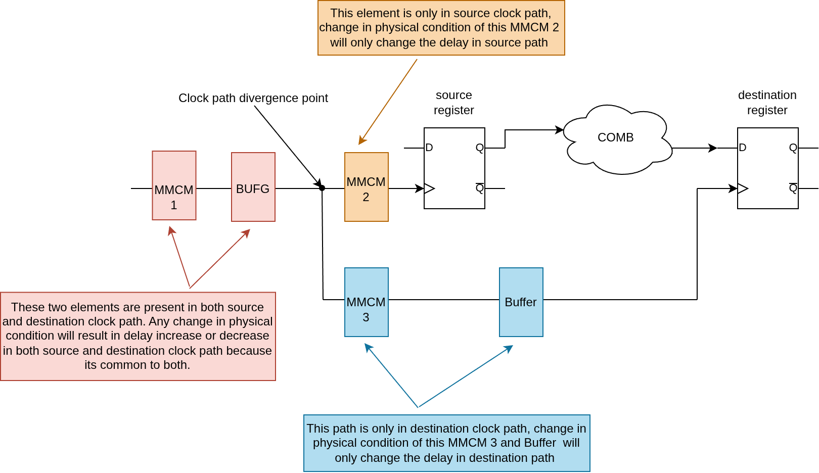
Figure 2: Detailed clock path showing common elements (MMCM1, BUFG) and path-specific elements
However, during slack analysis, if we consider the clock path delays for source and destination without considering the common path:
- It treats the shared portion as slow (max delay) for the launch path
- And at the same time as fast (min delay) for the capture path
This means that the same clock signal will reach the diverging point at different times. That cannot physically happen.
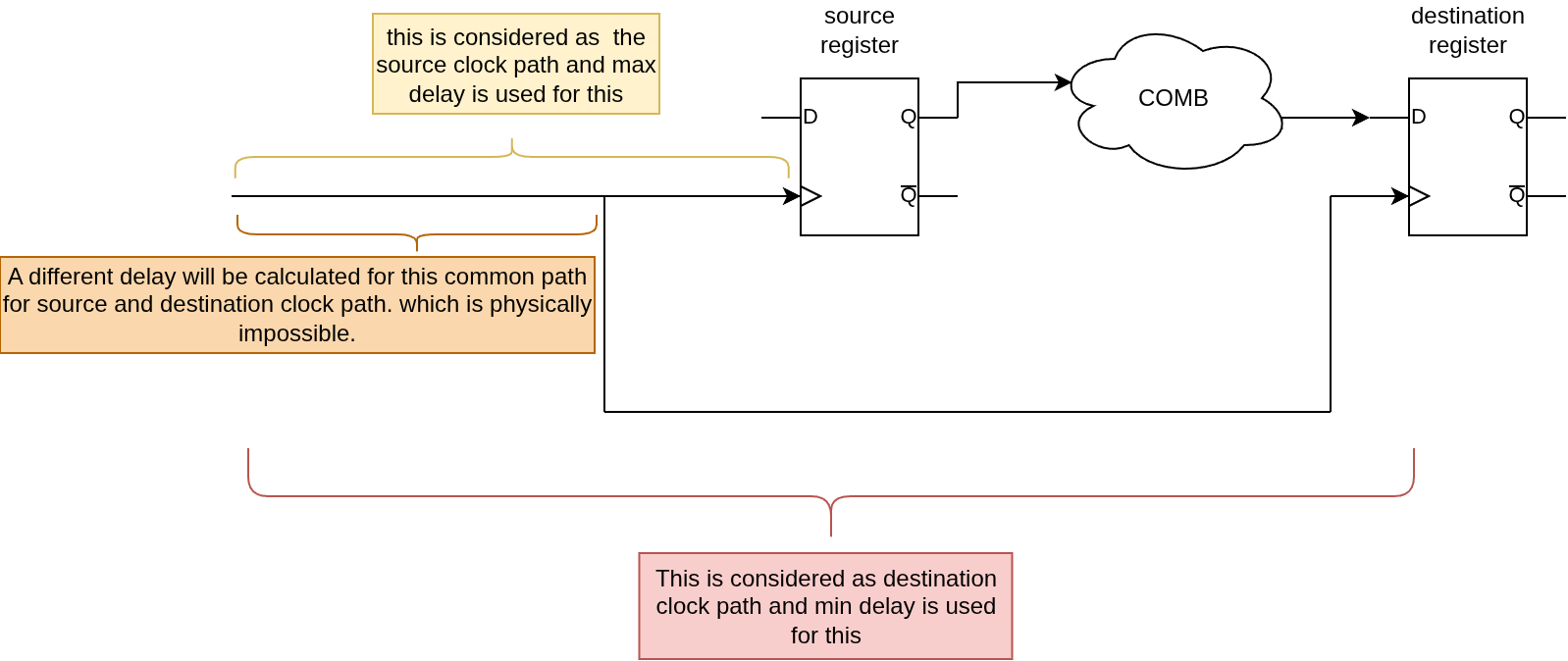
Figure 3: Clock delay calculation without CPR
The shared clock wire cannot be both slow and fast at the same time.
Physically, that common path will have one single delay value. By modeling it as max for launch and min for capture, the slack is reduced unnecessarily which does not represent the real slack. That artificial reduction is called clock pessimism. Clock Pessimism Removal (CPR) adds that unnecessary reduction back into slack.
To remove this unnecessary pessimism, Clock Pessimism Removal (CPR) is applied.
It is defined as:
\[CPR = D_{max} - D_{min}\]where:
- $D_{max}$ is the maximum delay of the common clock path
- $D_{min}$ is the minimum delay of the common clock path
This value represents the artificial difference introduced during worst-case modeling of the shared path.
In simple terms, we are adding back the delay difference that was subtracted unnecessarily from the common path during slack calculation.
2. Clock Skew
According to AMD Design Suite User Guide UG906:
Clock skew is the difference in insertion delay between the destination clock path and the source clock path. You measure it from their common point in the design to the endpoint and startpoint sequential cell clock pins, respectively.
So clock skew is the difference between clock edge arrival at the source register and the destination register. Clock skew compares the arrival of the same clock edge at two registers. This is different from setup analysis, which compares two different edges (launch and capture edges).
We know what skew is. But what is its importance? What does it tell us? To understand this we need to consider a few cases.
2.1 Negative Clock Skew
Means clock edge arrives at destination register earlier. Can cause setup violation as it will reduce the window available for data to settle down.
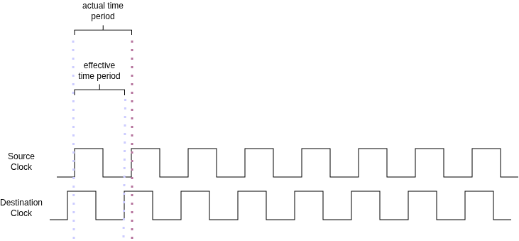
Figure 4: Negative clock skew: effective period is shorter than actual period
2.2 Positive Clock Skew
Means clock arrives earlier at source register. This is good for preventing setup time violation but this can cause hold violation as the clock arrives later at destination, giving not enough time for data to remain stable and meet hold time.
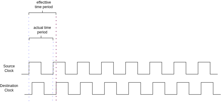
Figure 5: Positive clock skew: effective period is longer than actual period
2.3 Zero Clock Skew
Perfect scenario. No hold or setup violation due to clock skew.
2.4 Effect on Effective Clock Period
Clock skew basically changes the effective clock period. The effective clock period is the time interval between launch edge at source register and latch edge (edge next to launch edge) at destination register.
For positive clock skew, this effective period gets larger, as the latch edge takes more time to arrive at the destination register. Thus reducing the chance of setup violation as data gets more time to get stable and meet setup time.
For negative clock skew the effective clock period gets smaller, hence reducing the slack and increasing the chance of setup violation.
2.5 Clock Skew in Vivado
In Vivado clock skew is defined as:
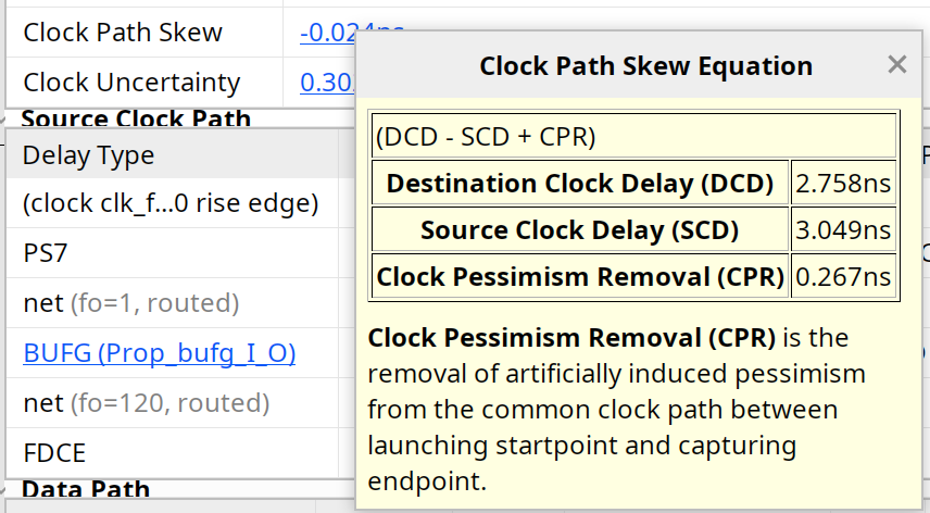
Figure 6: Clock path skew equation in Vivado
\[\text{Clock Skew} = DCD - SCD + CPR\]where:
- DCD = Destination Clock Delay
- SCD = Source Clock Delay
- CPR = Clock Pessimism Removal
Here’s a test, if you understand the previous section properly, you should be able to answer why CPR is added here.
3. Clock Uncertainty
Clock uncertainty deals with the uncertainty in the clock edge. It can be due to multiple causes as mentioned in the timing report:
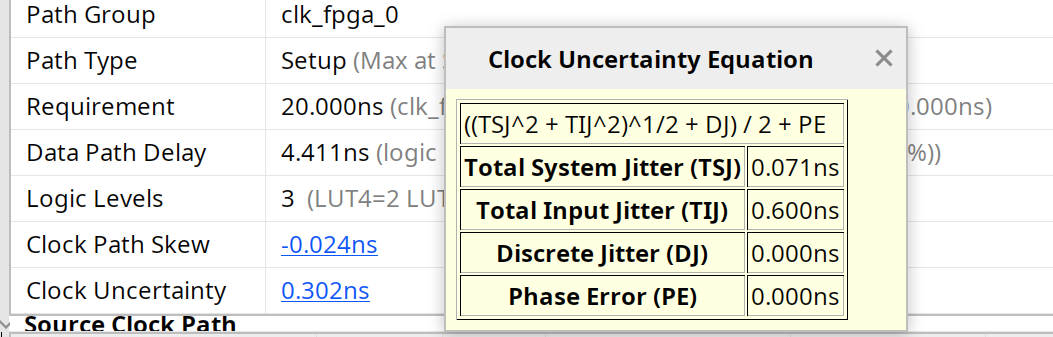 Figure 7: Clock uncertainty equation in Vivado
- Total System Jitter (TSJ): the uncertainty in the whole system due to physical variations. This would be the same for every path.
- Total Input Jitter (TIJ): The jitter present on the incoming clock signal before it enters the FPGA (from the external clock source). This would be added to only the path running on that external clock.
- Discrete Jitter (DJ): Deterministic, bounded jitter caused by predictable effects like duty-cycle distortion or periodic interference.
- Phase Error (PE): The static phase offset or alignment error introduced by clock management blocks like MMCMs or PLLs.
In Vivado, TSJ and TIJ are random jitter components, so they are combined using root-mean-square (RMS). TSJ, TIJ and DJ represents peak-to-peak variation, since we’re only interested in one clock edge and not both, it is divided by 2 to get the jitter of a single clock edge. Discrete Jitter (DJ) is deterministic i.e. no need for RMS as its not random, so it is added linearly before the division. Phase Error (PE), on the other hand, is a one-sided static phase offset introduced by clocking resources, so it is added directly and is not divided by 2.
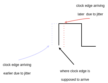
Figure 8: Effect of jitter on clock edge arrival time
For setup, uncertainty is subtracted from required time, because as mentioned before, we want to ensure the slack is positive even for worst case scenario. And subtracting the uncertainity means the clock edge arrives early at the destination register, hence reducing the available time for data to settle.
4. What’s Next
This wraps up our discussion on setup time anaylysis in Vivado. Next week, we’ll take a closer look at hold time analysis: how it differs from setup, and how Vivado reports it.
This is Part 2 of the Timing Analysis in Vivado series. Read Understanding FPGA Timing Analysis in Vivado: Part 1 if you haven’t already.