FPGA Timing Analysis in Vivado: Setup Slack
1. Introduction
One of the most daunting topics when starting out in the FPGA domain is timing analysis. Before jumping into techniques for solving timing violations, we need to understand how to perform timing analysis, what information the tools give us, and how to interpret it.
Two fundamental concepts in digital design are setup time and hold time. When targeting a specific clock frequency, we must ensure that the design meets both of these timing constraints. In this post, we’ll focus on meeting setup time requirements, specifically for register-to-register (reg-to-reg) paths. The goal is to ensure that the data has enough time to propagate and stabilize at the destination register before the capturing clock edge arrives.
2. Key Concepts
A reg-to-reg path is simply the path between two registers: a source register that launches the data, and a destination register that captures it.
A few terms we’ll use throughout this post:
- Launch edge: The clock edge at which the source register launches data. We treat this as our reference point (time = 0).
- Latch edge: The clock edge at which the destination register must capture the launched data. For a single-clock design, this is one clock period after the launch edge.
- Source clock path: The route taken by the clock signal to reach the source register’s clock pin.
- Data path: The route taken by the data from the source register’s output (Q) to the destination register’s input (D).
- Destination clock path: The route taken by the clock signal to reach the destination register’s clock pin.
- Tcq (Clock-to-Q delay): The delay from the clock edge at the source register to when valid data appears at its Q output.
- CPR (Clock Pessimism Removal): A correction factor that accounts for overly pessimistic analysis on shared clock path segments. We’ll cover this in detail in a later post.
- Clock uncertainty: Accounts for jitter and other variations in the clock signal. Also covered in a later post.
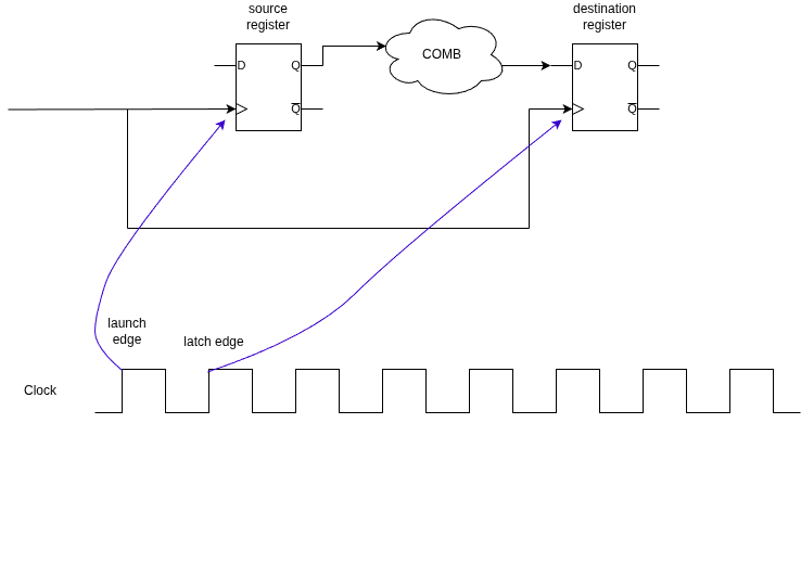
Figure 1: source/destination register and launch/latch clock edge
3. Viewing Timing Paths in Vivado
To inspect a reg-to-reg setup timing path in Vivado, open your implemented design and navigate to Timing → Intra-Clock Paths. Double-click on the path you want to analyze. You should see something like this:
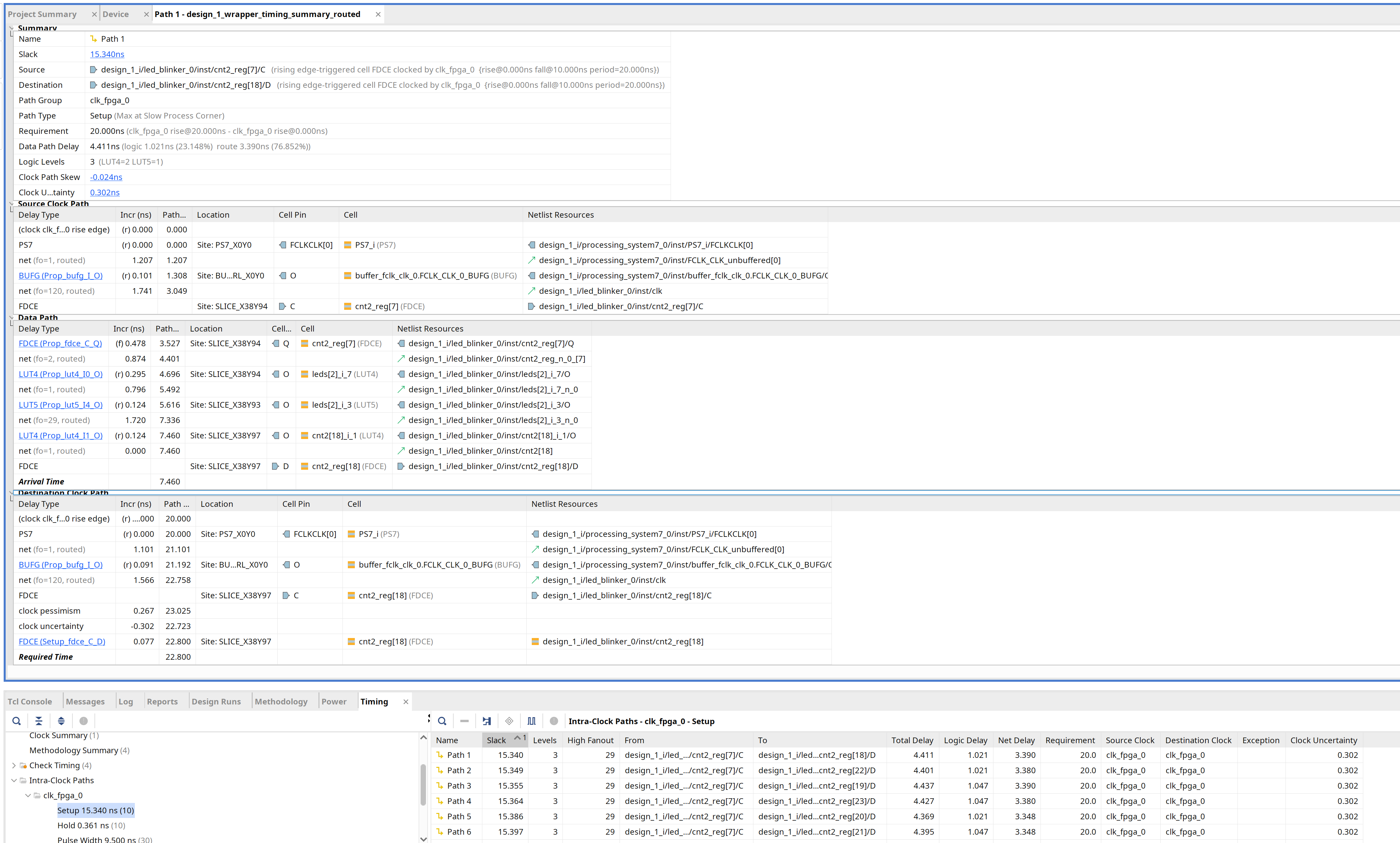
Figure 2: Timing path window in Vivado
Notice the “From” and “To” tabs. “From” shows the source register, and “To” shows the destination register. This view is available for every path in the design and can be inspected individually.
4. Understanding Slack
At the top of the path view, just below the path name, you’ll see the slack value. Click on it to see how it’s calculated:
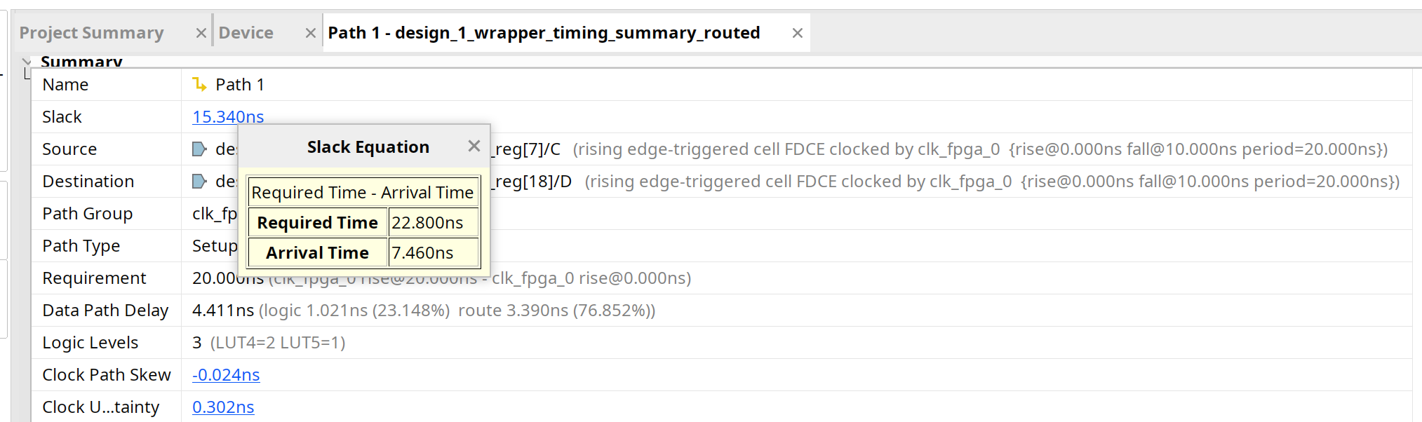
Figure 3: slack calculation equation
The slack formula is straightforward:
Setup Slack = Data Required Time − Data Arrival Time
If the slack is positive, timing is met i.e. data arrives and settles before the capturing edge (with margin to spare). If the slack is negative, you have a timing violation i.e. data doesn’t arrive in time, and the design won’t reliably work at that clock frequency.
Let’s now break down how Vivado calculates the arrival time and the required time.
5. Breaking Down the Timing Path
5.1 Source Clock Path
The source clock path is the route the clock takes from its origin to the clock pin of the source register.

Figure 4: Source clock path delay breakdown
In the Vivado report, the “Incr” column shows the delay contribution of each component along the clock’s path. For example, if BUFG shows an increment of 0.101, that means the global clock buffer adds 0.101 ns of delay. The “Path” column gives the running total. So if the final entry in the Path column reads 3.049 ns, that’s the total source clock path delay.
5.2 Data Path
The data path covers everything between the source register’s Q output and the destination register’s D input. This includes the Tcq delay of the source register, any combinational logic, and the routing between them.
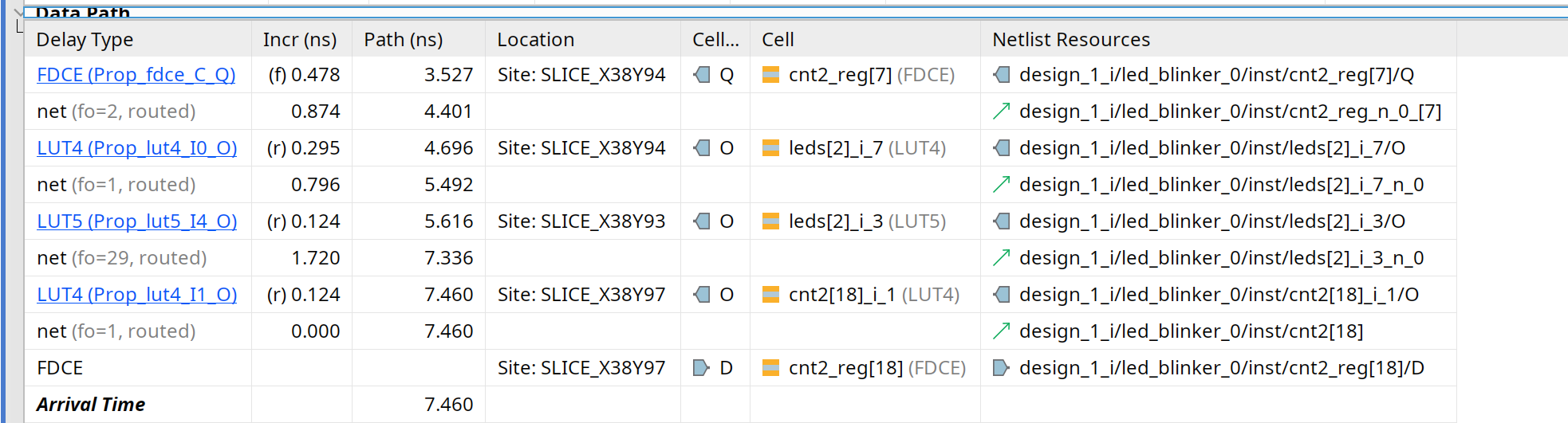
Figure 5: Data path delay breakdown.
One thing that might confuse you: the cumulative delay in the Path column doesn’t start from zero. It picks up where the source clock path left off. That’s because the arrival time is computed as the sum of the source clock path delay and the data path delay:
Arrival Time = Source Clock Path Delay + Data Path Delay
So the final row in the data path section gives you the total arrival time directly. If you want just the data path delay by itself:
Data Path Delay = Arrival Time − Source Clock Path Delay
5.3 Destination Clock Path
The destination clock path is the route the clock takes to reach the destination register. Vivado uses this to calculate the required time i.e the maximum time data can take to arrive at destination register.

Figure 6: Destination clock path and required time calculation
The calculation starts from the latch edge. For a 50 MHz clock (period = 20 ns), the latch edge sits at 20 ns. From there, Vivado adds the destination clock path delay and applies corrections for clock pessimism removal (CPR) and clock uncertainty. It also accounts for the setup time of the destination register.
6. A Note on Negative Setup Time
You might notice something odd in Vivado’s required time calculation: the setup time appears to be added rather than subtracted. Intuitively, we’d want to subtract it, as data needs to arrive some time before the clock edge, so subtracting setup time from the required time should make the constraint tighter.
The reason is that setup time in Vivado can be both positive and negative. For most registers it’s positive. But for some cells, the setup time is actually negative. Positive setup time means data needs to be stable for the setup time before the clock edge. However, if setup time is negative, then it means that the data can arrive that much time after the clock edge and it will still be caputured correctly. In Vivado if setup time is postive than it means it should be added in required time and if negative then it should be subtracted.
There’s a good thread on this on the AMD support forum: https://adaptivesupport.amd.com/s/question/0D54U00008CQt22SAD/data-required-time-and-setup-time
7. Putting It All Together
Here are the two core formulas that drive setup timing analysis:
Data Arrival Time = Launch Edge + Source Clock Delay + Tcq + T_datapath
Data Required Time = Latch Edge + Dest Clock Delay − Setup Time + CPR − Clock Uncertainty
Where:
- Launch Edge: 0 ns (our reference point)
- Latch Edge: One clock period after the launch edge (e.g., 20 ns for a 50 MHz clock)
- Source Clock Delay: Total delay from the clock source to the source register’s clock pin
- Tcq: Clock-to-Q delay of the source register
- T_datapath: Combinational + routing delay from source Q to destination D
- Dest Clock Delay: Total delay from the clock source to the destination register’s clock pin
- Setup Time: Setup time requirement of the destination register (can be negative)
- CPR: Clock Pessimism Removal — corrects for shared clock path pessimism
- Clock Uncertainty: Jitter and other clock variations
And the final check is simply: if the required time minus the arrival time is positive, your setup timing is met.
8. What’s Next
This covers the basics of reading and understanding setup timing reports in Vivado. In the next post, we’ll dig into clock pessimism removal, clock uncertainty and clock skew. Specifically, what they are, how are they calculated, and why they matter.