Reg-to-Pin Timing Analysis
1. Introduction
So far, we have been looking at timing analysis for paths entirely inside the FPGA known as reg-to-reg paths. But those are not the only paths that exist in a design. When a signal enters an external FPGA pin or leaves through one, reg-to-reg analysis methods are no longer applicable. For such cases, we use pin-to-reg and reg-to-pin paths.
As the names suggest:
- Pin-to-reg: An input signal arrives from an external pin and is captured by a register inside the FPGA.
- Reg-to-pin: An output from a register inside the FPGA drives an external pin, which in turn feeds a register in an external device.
For now, we will focus on the reg-to-pin path.
2. The Reg-to-Pin Path
In a reg-to-pin path, the source register is inside the FPGA, but the destination register resides in an external device i.e. a memory chip, ADC, DAC, or any other peripheral on the board. The data travels from the source register through the FPGA’s internal routing, out through the FPGA output pin, across the PCB trace, and finally into the destination register of the external device.
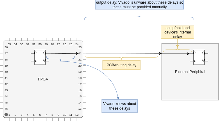
Figure 1: Reg-to-pin path to the external device
3. Output Delay and Why It Is Needed
Vivado can fully model all delays internal to the FPGA i.e. from the source register’s clock-to-output time through the internal routing to the output pin. What it cannot account for on its own is what happens beyond that pin. The delays it cannot see include:
- PCB trace propagation delay
- Setup time requirement of the external device
- Hold time requirement of the external device
We need to supply these values manually so that Vivado has a complete picture of the path and can run a meaningful timing analysis. This is done through the output_delay constraint, whose value comes from the external device’s datasheet (for setup and hold times) and the board layout (for PCB trace delay).
As with all delays, these values vary across process, voltage, and temperature (PVT) corners, so output_delay has both a maximum and a minimum value:
Note that output_delay_min can be negative when the minimum PCB delay is smaller than the external device’s hold requirement.
For example:
\[T_{hold,\,ext} = 2\ \text{ns}\] \[T_{pcb,\,min} = 0.5\ \text{ns}\]The external device needs data stable 2 ns after the clock edge, but the board only provides 0.5 ns of natural delay — so the FPGA must “hold” the data longer. The constraint becomes: \(\text{output_delay}_{min} = T_{pcb,\,min} - T_{hold,\,ext} = 0.5 - 2 = -1.5\ \text{ns}\)
4. Timing Equations for Reg-to-Pin
4.1 Data Arrival Time
Vivado computes the data arrival time as the time the data takes to travel from the launch clock edge to the FPGA output pin:
\[T_{arrival} = T_{clk,\,launch} + T_{co,\,max} + T_{route,\,int} \tag{3}\]$T_{co,\,max}$ is the maximum clock-to-output delay of the source register and $T_{route,\,int}$ is the internal routing delay from the register to the output pin.
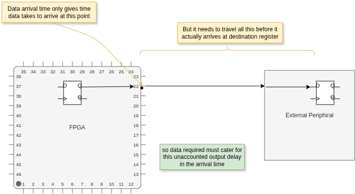
Figure 2: Vivado’s visibility of paths
4.2 Data Required Time — Setup Analysis
For the data to arrive at the external device’s destination register in time, it must be present at the FPGA output pin early enough to still travel across the PCB and satisfy the external setup requirement. The data required time at the output pin is therefore:
\[T_{required} = T_{period} - \text{output_delay}_{max} - \text{clock uncertainty} \tag{4}\]Subtracting output_delay_max pushes the required time window earlier, forcing the timing analysis to ensure that data out of the FPGA pin has enough time to cross the PCB and meet the external device setup time before the next capture edge. The setup slack is:
4.3 Hold Analysis
For hold timing, the minimum delay path is analysed using output_delay_min.
The hold slack is:
\[\text{Slack}_{hold} = T_{arrival,\,min} - T_{required} \geq 0 \tag{7}\]where $T_{arrival,\,min}$ uses the minimum clock-to-output and minimum internal routing delays. Since output_delay_min can be negative, the hold constraint is less restrictive in such cases.
One thing worth noting is that there is no CPR in these equations. That is because the clock is external — both source and destination clock paths are independent without any shared segment. Also, the destination clock delay is 0 in the timing report, as the clock path is external to the device and Vivado has no visibility of it.
5. Applying the Constraint in Vivado
The output_delay constraint is applied using the set_output_delay command. It can be written directly in the .xdc file or generated through the Vivado GUI. The GUI method is shown below.
5.1 Step-by-Step: Using the Vivado GUI
Step 1. After synthesis, open the synthesized design from the Flow Navigator and click on Edit Timing Constraints.
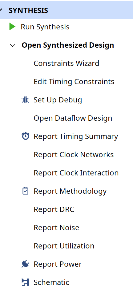
Figure 3: Vivado Flow Navigator — navigate to Open Synthesized Design → Edit Timing Constraints.
Step 2. In the Timing Constraints window, double-click on Set Output Delay. The configuration dialog shown in Figure 4 will open.
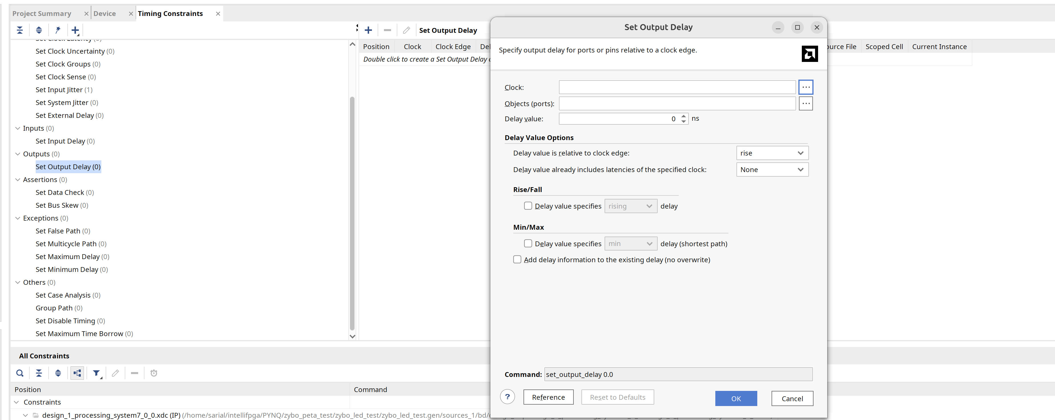
Figure 4: Set Output Delay dialog in Vivado.
Step 3. Click the … button next to Clock. In the Specify Clock dialog, click Find to list all available clocks in the design. Select the clock that drives the source register and the external peripheral, move it to the selected list using the right-arrow button, and click OK.
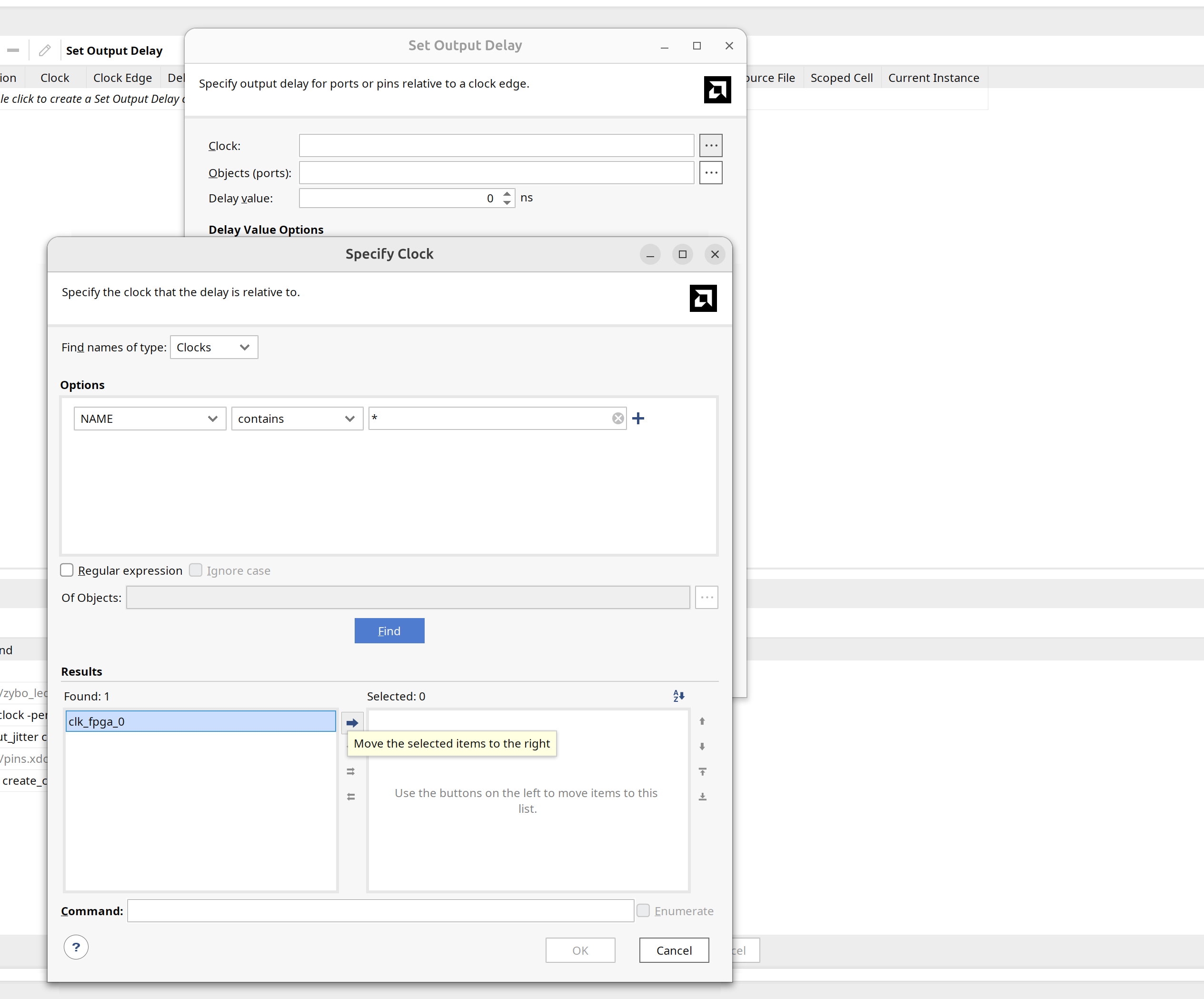
Figure 5: Specify Clock dialog.
Step 4. Click the … button next to Objects (ports). In the Specify Delay Objects dialog, click Find to list the available output ports. Select the ports you want to constrain and click Set. If you previously added some ports and want to add more, use Append instead, so the existing selection is not overwritten.
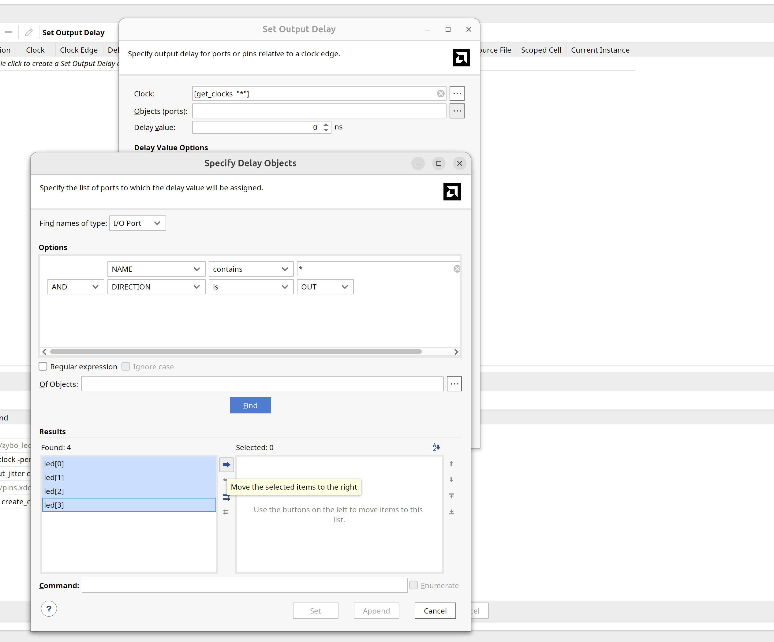
Figure 6: Specify Delay Objects dialog.
Step 5. Configure the delay options in the dialog:
- Delay value: Enter the output delay value in nanoseconds. This value is relative to the capture clock edge at the external device. A positive value means the data must be present at the FPGA output pin at least that much before the capture edge — the typical case for setup, since both the PCB delay and the external setup time eat into the available clock period. A negative value appears in hold analysis when the minimum PCB trace delay exceeds the external device’s hold requirement.
- Delay value is relative to clock edge: rise for rising-edge capture, which applies to the vast majority of designs.
- Min/Max: Set to max for setup analysis and min for hold analysis.
- Rise/Fall: Enable only when PCB traces have noticeably different propagation times for rising and falling edges — for example, due to pull-up/pull-down resistor networks or open-drain outputs. In most standard designs, leave this unchecked.
- Delay value already includes latencies: This controls whether the clock latencies modelled internally by Vivado (source and/or network latency) are already embedded in the delay value you are entering. In almost all standard FPGA designs, this should be left as None, allowing Vivado to add its internal clock latency on top of the specified output delay. Only change this in advanced scenarios where clock latencies are manually specified with
set_clock_latency.
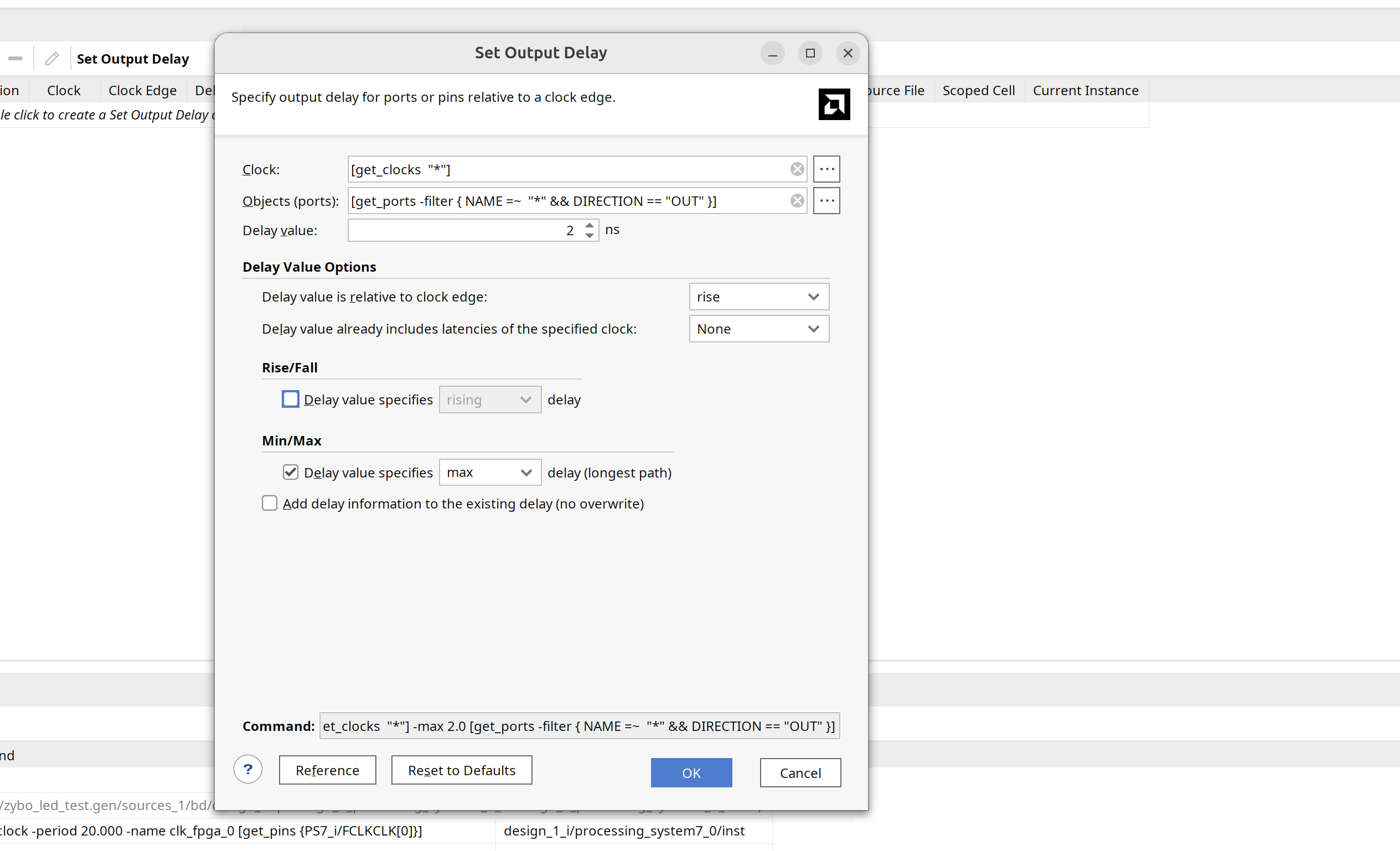
Figure 7: Completed Set Output Delay dialog configured for setup analysis.
Step 6. Click OK and press Ctrl+S to save. Vivado will write the corresponding set_output_delay entry into the XDC file. Repeat the above steps for hold time analysis, setting Min/Max to min and entering the appropriate (typically negative) delay value.
5.2 Generated XDC Constraints
After completing both the setup and hold configurations, the XDC file will contain entries similar to those shown in Figure 8.

Figure 8: Generated set_output_delay constraints in the XDC file.
After synthesis, in the Setup analysis window, the output delay is subtracted from the required time:
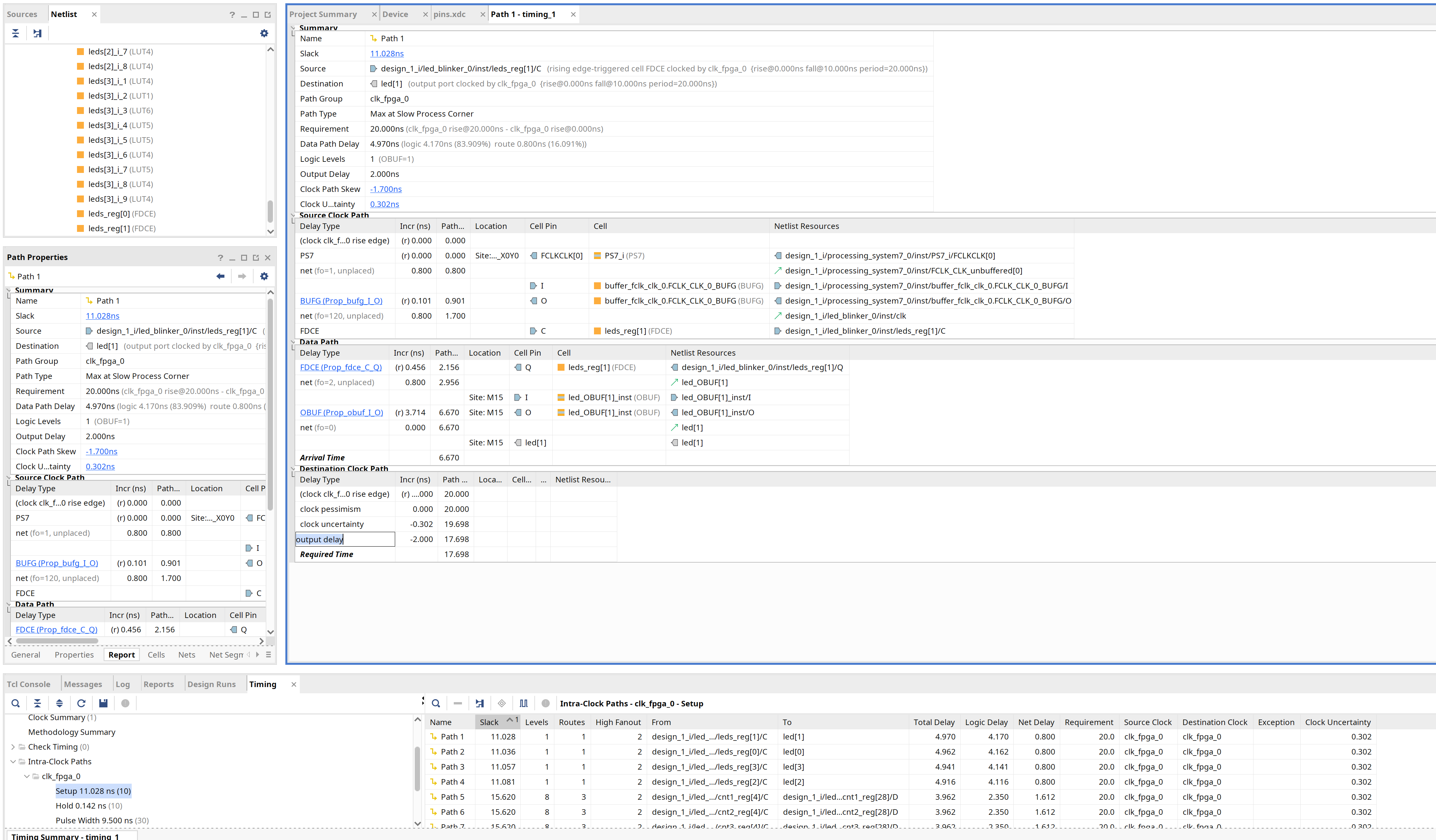
Figure 9: Setup Path window for Reg to pin path.
And added to the required time in hold analysis:
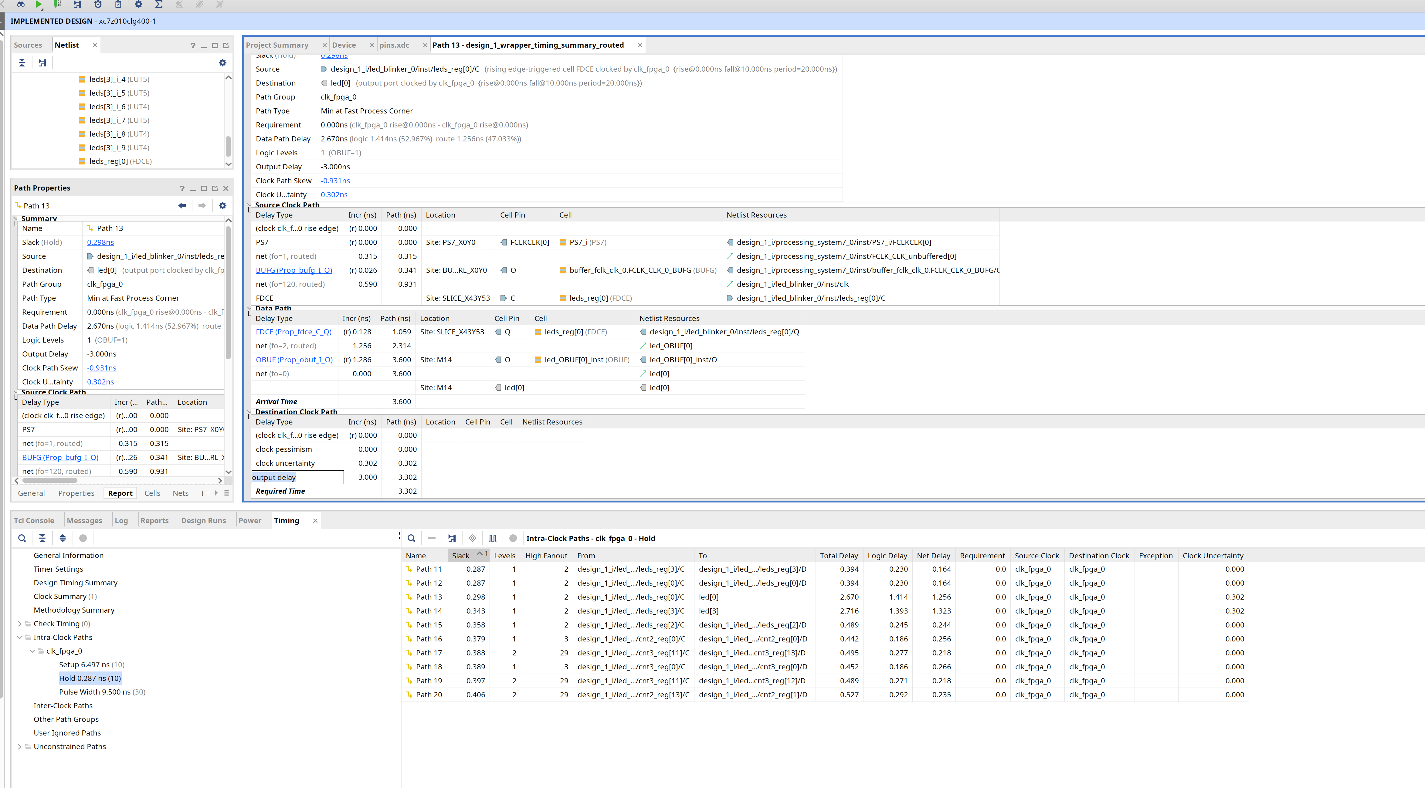
Figure 10: Hold Path window for Reg to pin path.
6. What’s Next
In this post we covered the reg-to-pin direction — data flowing out of the FPGA to an external device. The complementary case is pin-to-reg: data arriving into the FPGA from an external pin and being captured by an internal register. In the next post we will look at how to model that path, how set_input_delay works, and how the arrival and required time equations change when the launch register is outside the FPGA.
Blogs in this Series: Understanding FPGA Timing in Vivado
Part Topic Part 1 Setup Analysis Basics — Arrival Time, Required Time, Slack Part 2 Clock Pessimism Removal, Clock Uncertainty & Clock Skew Part 3 Hold Analysis Part 4 (this post) Reg-to-Pin Timing & Output Delay Constraints